I have blogged here and here outlining an industrial policy to promote domestic innovation in electronic products. The policy should identify a few (say, 3-5) products and encourage phased localisation over a five-year policy regime using a combination of targeted incentives and mandates.
No product is more appropriate for such a policy than smart meters, on which India has launched a massive scheme (the RDSS) to replace the existing 200-250 million electromechanical and basic digital meters with bidirectional prepaid meters by the end of 2028. This amounts to almost a 10-year Rs 2.4 - 3 lakh Cr contract. Given that almost all meters are procured by government-owned discoms with the central government subsidy under RDSS, it is a perfect opportunity to use incentives and mandates.
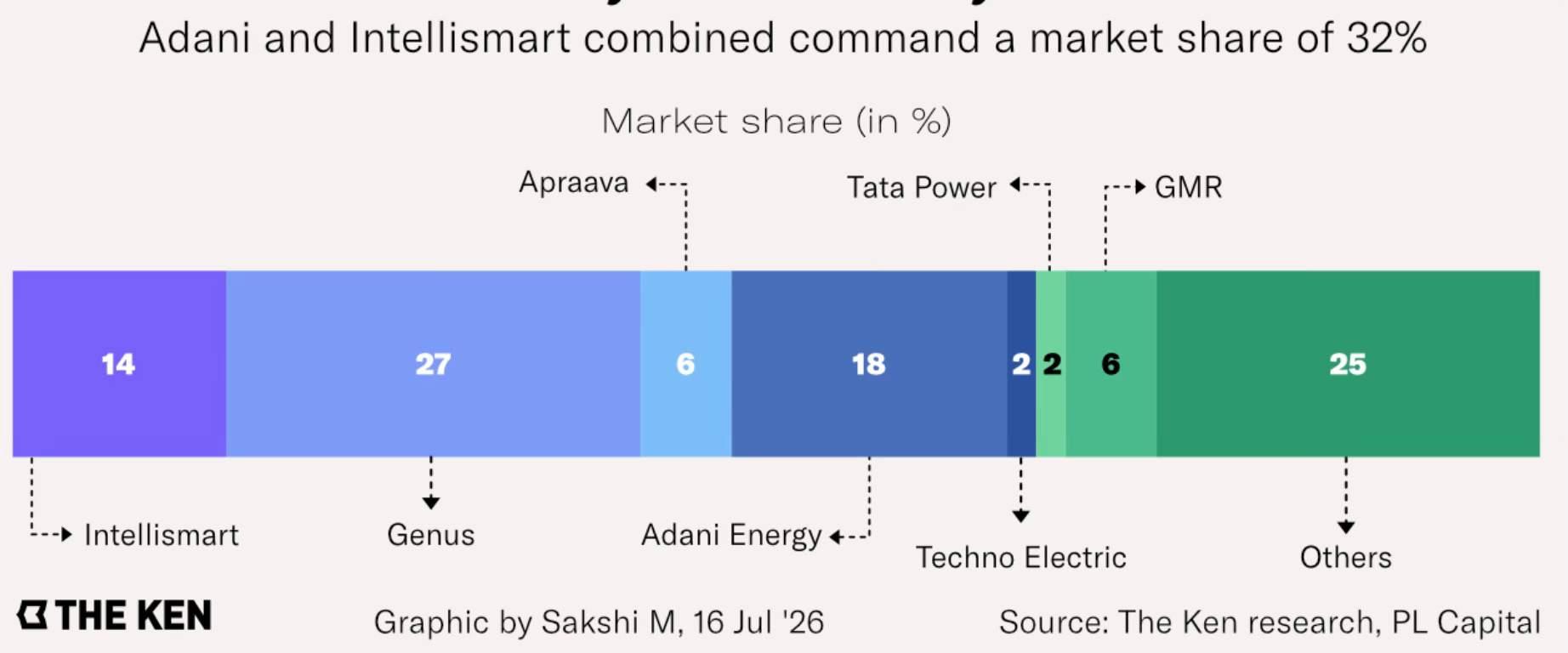
The meters are rolled out largely on a TOTEX model, where private Advanced Metering Infrastructure Service Providers (AMISPs) finance, install and operate the meters over 8-10 year contracts, paid per meter per month (of around Rs 60-80). The AMISPs, in turn, procure the meters from OEMs like Secure Meters, HPL, Schneider, Landys+Gyr, and Genus. The major AMISPs are Adani Energy, Intellismart (now purchased by Adani Energy), Genus, GMR, Tata Power, and Techno Electric. This market concentration, on both the AMISPs and the meter manufacturers, while a risk, also makes it easier to implement any phased localisation policy.
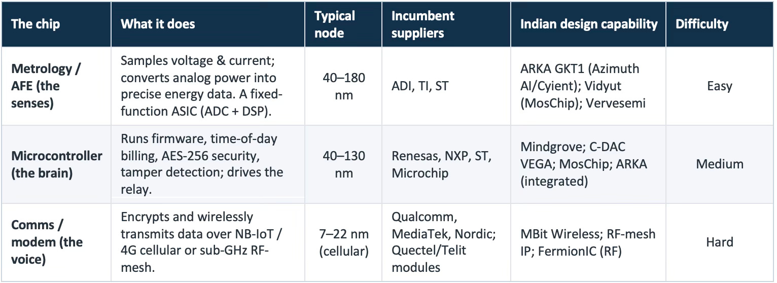
The smart meters are currently assembled in India, with all three major components being sourced externally from foreign suppliers. In terms of its technology, a smart meter is a rugged, always-on computer with three core integrated circuits (plus a latching relay, which is an electromechanical switch rather than a chip). They are the metrology IC (the sensor), the microcontroller unit (MCU) (the brain), and the modem (the voice) of the meter, and they differ sharply in complexity, which makes a phased localisation strategy possible.
Fortunately, India has a few chip design startups who have already commercialised the metrology-plus-processing layer, and with credible domestic microcontroller unit design. The narrowband IoT/4G baseband for the modem is a genuinely hard one, though achievable in a phased manner given the commercial incentives that come with a policy.
The table captures the smart meter components and the current market landscape.
I have blogged here highlighting the entry barriers arising from financing challenges and deployment opportunities (given the lack of Indian OEMs) for indigenous chip design firms to break out in the chip design market. In this context, the massive volume of subsidised smart meters procured by discoms is an unmatched deployment breakthrough for the domestic chip design industry.
This opportunity can be harnessed through a general “product-mission industrial policy” built on four levers: aggregate demand, mandate and phase, bridge OEMs to chip firms, de-risk capital. The 200 million meters (≈600 million chips) is the rarest asset in industrial policy: demand that is enormous, captive, and shaped by the state itself. India is already partway there, having commercialised indigenous meter silicon (Azimuth AI’s ARKA GKT1 and MosChip’s Vidyut).
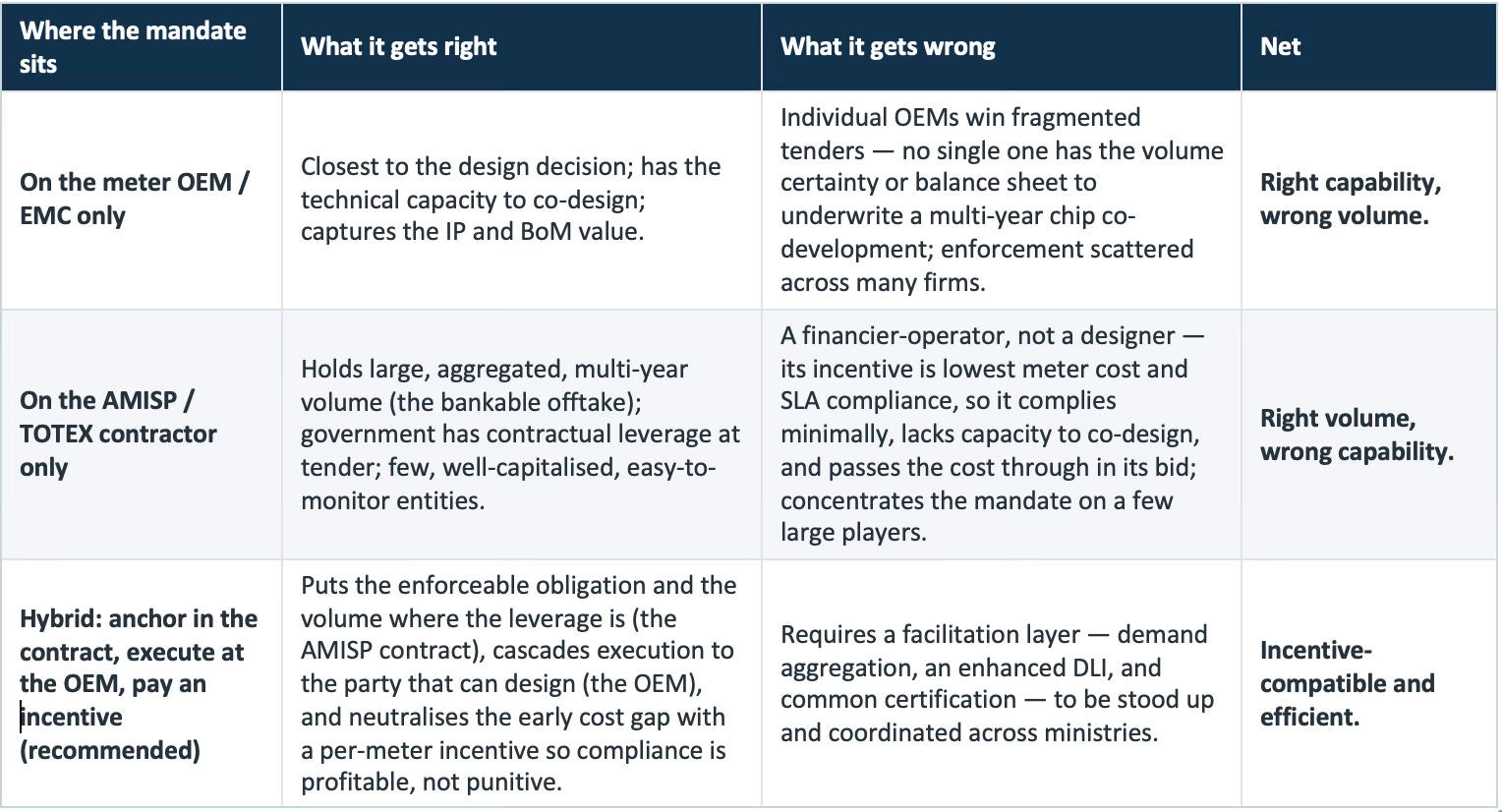
There are two commercial firms in the smartmeter contract - the AMISPs and the meter OEM. The two parties hold complementary assets - the AMISP holds the bankable multi-year volume and the government’s contractual leverage; the meter OEM holds the design capability and intellectual property (IP). The most incentive-compatible contracting arrangement would be to anchor the mandate in the AMISP/TOTEX contract, cascade execution to the OEM, and pay a per-meter incentive that neutralises the early cost gap. An OEM-only mandate fails on volume, and an AMISP-only mandate fails on capability and gets passed through as cost.
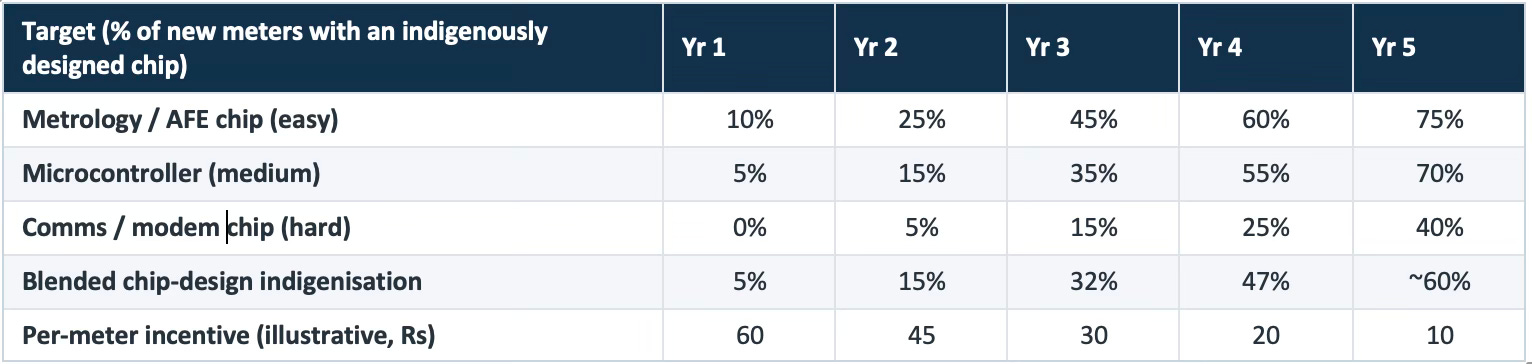
An illustrative localisation phasing and incentivisation is indicated, which would amount to a total subsidy of Rs 1000-1200 Cr, or less than 0.5% of the total project cost and about $1.6 billion of total chip cost over 5 years. The per-meter incentive neutralises the early cost gap, and it tapers off as volume rises. This would amount to localisation of 60% of the chip design for smartmeters. The numbers could be tweaked and finalised after consultations involving all stakeholders - OEMs, AMISPs, and chip design startups.
I am assuming only the localisation of the chip design, and not the fabrication (amounting to about 60% of the chip cost), thereby enabling domestic capture of about $1 bn of chip value besides the development of invaluable chip design capabilities at scale. However, the central government could target even the fabrication of the higher-nanometer chips under the Semiconductor Mission. At the least assembly, testing and packaging (ATMP) could be localised in parallel.
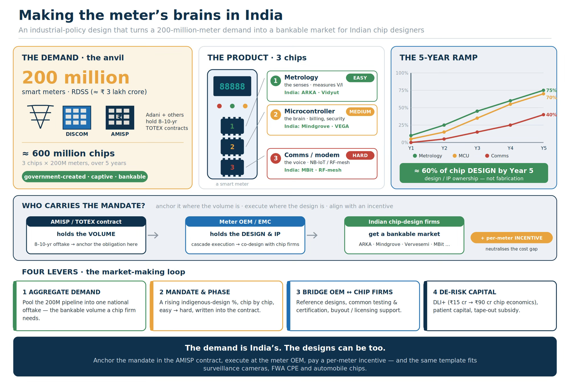
This would be a genuinely end-to-end localisation achievement that can be emulated for certain other products like surveillance cameras, Fixed Wireless Access (FWA) and other customer premises equipment, automotive chips, etc.
The details are important. The target is chip design - ownership of the IP and the front-end engineering - not fabrication. An Indian-designed metrology or MCU chip can be fabricated at a foreign foundry (TSMC, UMC) or, increasingly, at an Indian one (Tata-PSMC, and the Micron and Kaynes/CG packaging lines) and still deliver the objectives of domestic IP, design jobs, security assurance and value capture. Fabrication indigenisation is a different decade-long, capital-intensive problem, albeit achievable now in some degree with the Indian Semiconductor Mission (ISM). For a country which originates 30-40% of the world’s chip-design talent, this is the natural place to start.
To prevent gaming and ‘badge engineering’, ‘indigenously designed’ must be defined tightly - the IP is owned by an Indian entity and the RTL design and tape-out are done in India, verified by a third party - and not an imported design with a domestic label.
The biggest challenge would be to support the domestic startups quickly build design and testing capabilities to meet the large volumes they must commit (including the continuous technology and standards updations). This will require the OEMs and AMISPs working closely with the chip design startups. They could offer some form of advance market commitments to the chip design startups that would allow them the runway to raise capital and finance their rapid capabilities development.
The success of this will depend on its ownership by the Ministry of Power, which would need to work closely with the Ministry of Electronics and Information Technology, which currently run the electronic products and components schemes and the semiconductor mission.
As an important requirement, there should be no relaxation of the quality and standards requirement from the domestic chip designers. They should pass the same accuracy and reliability tests required by incumbents. In fact, they (either directly or through the meter makers) should also be nudged with soft targets on exports so as to create the incentives for maintaining global competitiveness. If they are unable to with all the support, then perhaps it might be justifiable for the government to throw up its hands and reconcile itself to the quality of Indian entrepreneurship.


No comments:
Post a Comment