Given its massive capital requirements, amounting to several billions of dollars, and highly specialised manufacturing ecosystem, establishing semiconductor chip fabrication facilities in India poses several insurmountable challenges. In the circumstances, and also given its far lower capital requirements and the country’s comparative human capital advantages (it is estimated that 30-40% of global chip design talent is Indian) in software development, it has been suggested that India should focus on fabless chip design.
There is no doubt that there are Indian startups with the requisite expertise and talent to design chips and products. But there are perhaps two binding constraints to the emergence of chip and product design companies in India – its acutely deficient risk funding ecosystem and, more critically, the absence of domestic companies (OEMs, etc.) that can deploy these designs in their products.
I blogged here on industrial policy for semiconductor chips.
Semiconductor chip design and manufacturing are among the most daunting of industrial activities. This sums up the complexity.
A typical integrated circuit chip can involve over 500 distinct production stages and cross as many as 70 international boundaries before it reaches the consumer. Across this complicated global supply chain, the scale of interdependencies is vast: China has a monopoly over certain critical minerals, the US and UK have a combined monopoly over chip design tools, and so on. Moreover, there are dozens of hyper-specialised suppliers spread across the world who hold virtual monopolies over critical process technologies needed to manufacture chips. They can act as technological ‘choke points’.
Underlining the complexity, it must be noted that semiconductor chips are perhaps the only major area where China has struggled to make much headway despite spending hundreds of billions of dollars. Apart from the high-end chips fabrication, the biggest challenge is with chip manufacturing equipment, which is dominated by the US and Japan, and where China is a marginal player despite being the largest buyer.
Tracxn has estimated 117 semiconductor chip design firms in India by the end of 2024. The Design-Linked Incentive (DLI) scheme of the MEITY, introduced in 2021, had an allocation of just Rs 1000 Cr (of the total of Rs 76,000 earmarked for semiconductors) to nurture 100 chip design companies over five years and ensure at least 20 such companies have a turnover of Rs 1,500 Cr or more. The maximum funding available to a firm is Rs 15 Cr.
This has proved inadequate since it requires at least $10 million (Rs 90 Cr) to build even a basic chip, much less the several tens of millions for a more sophisticated chip. Just licensing the IPs required to design a chip alone will cost a few million. Private sector funding, too, has been scarce.
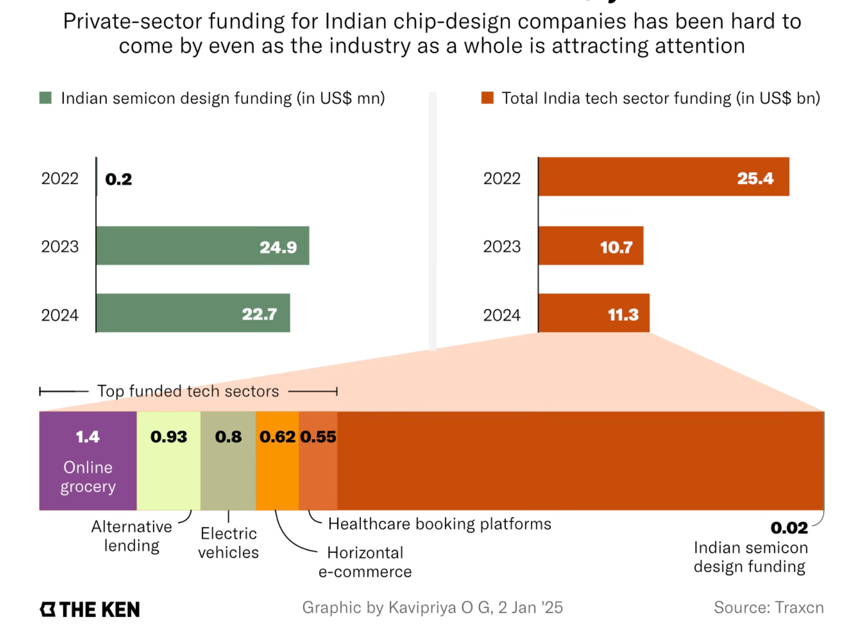
Similar levels of funding are calculated from other sources (and this) too. In 2024, seven chip design startups raised $28 mn.
The analysis of funding shows that most of the deals are seed or pre-seed stage, with just one or two in the pre-Series A or Series A stages.
The Ken has a very useful interview with P Raja Manickam, former head of Tata Electronics’ outsourced services unit, where he describes how China entered the semiconductor market.
The Chinese government arm-twisted Qualcomm and said, “Look, I’m giving you this huge market in cell phones. You’re selling to Huawei, Oppo, Xiaomi, and others. I have a fab; you build those chips here, at least some of the lower end stuff.” As a result, Qualcomm now has quite a bit of business with SMIC. China didn’t stop with that; they said now that you are building the wafers, also do the packaging in China. Qualcomm is not a manufacturing company, it could have said, “We don’t do packaging. We just give it to somebody else.” But China forced them to bring a supplier, Amkor [Technologies], and invest in them just to fulfil the Chinese demand. So, the thought process is this: if we have a fab in India, we could do the same and go to Qualcomm. And I think it makes sense now because Qualcomm is searching for a market. They’re getting thrown out of China.
He divides the global wafer market into three categories - 30% going to memory, 30% to the 3-4 nm chips (a few products made by very few companies); and the 40% going to mass market electronics (microcontrollers, MOSFETs, DC/AC converters etc.) which largely sit in the 130-180nm range.
Manickam describes why despite the presence of over 50,000 chip designer engineers working in India, Indian firms and startups struggle to develop products.
One, the experience of building a product company did not exist in India. Just because you are a designer in a TI or a similar company doesn’t mean that you know how to build a company… Even if you work for these companies in India, you will never be able to make an entire chip. They certainly don’t expose you to marketing and selling and all such aspects. Secondly, the moment you finish your design and ship it to Taiwan or some other fab, your door closes. You have no idea how to work with TSMC or how to get the product done. And that is why I always say we need a fab in India. You can never build a product company without a fab. Why is Taiwan successful? A small country with very few people. Look at Mediatek (a Taiwanese fabless semicon firm); they gave Qualcomm a run for the money… they can compete with TI sitting in Taiwan because they have access to the fab. They can tweak their process with the fab. A lot of startups in Taiwan come from TSMC, not from design companies… Startups create some IP, run out of cash, and VCs never invest in these guys because they don’t see them becoming a hundred-million or a billion-dollar company. So, they sell their IP to somebody.
The lack of large firms and an ecosystem, and the stranglehold of majors, also mean that Indian chip design firms spend 50-80% more for taping out chips than their counterparts elsewhere, like NXP Semiconductors.
Skilled manpower is a major constraint. A Ken report states that the $115 bn electronics manufacturing sector in India is expected to touch $500 bn by FY30. It is expected to create about 12 million jobs over the next two years across operational roles like technical troubleshooting, electronics design, running Surface Mount Technology (SMT) lines, and operating CNC (computerised numerical control) machines. The report also points to a Teamlease finding that at least 10 million of these potential hires may lack relevant practical skills.
Skills necessary to run electronics production lines and semiconductor operations are rarely taught in the current academic curriculums… Not many would know how a printed circuit board works or what a 3D laser inspection is… In mid-2023, Macdermid Alpha set up a production line for components at IIT Madras where students can get hands-on training to develop necessary skills. Bhatkal was inspired by similar models in US universities, like the Georgia Tech Manufacturing Institute in Atlanta. The motive was simple: upskill the talent so their recruiters could cut down on the time and resources spent on training them… The institute runs an 11-day workshop, which is open to students from the Industrial Training Institute (ITI) and even employed engineers who want to upgrade their skills… So far, over 340 students have completed the training and found jobs at various companies—the likes of autocomponent maker Uno Minda, printed-circuit-assembly maker Syrma SGS, and even one of the Tata group companies… Macdermid runs a similar course at the College of Engineering, Pune, in partnership with two-wheeler maker Bajaj Auto and US-based electronics manufacturer Jabil. NMTronics, a Noida-based electronics-solutions provider, also runs one at IIT Kanpur… it cost companies nearly Rs 4–5 crore ($466,000–582,000) to set up each of these centres.
This article about getting Micron to establish a chip ATMP facility at Sanand in Gujarat points to the challenges associated with attracting such investments, even with 70% of the $2.7 billion investment being a public subsidy.
What does all this mean for the development of India’s chip design market?
The US semiconductor chip industry has developed on the back of seed grant financing of hundreds of startups by the government and plentiful VC funding of promising startups. Two critical factors contributed to the success of this strategy: the presence of deep and risk-taking VC investors and OEMs with a massive volume of demand for these chips and designs. Since neither of these two factors is available in India, Indian chip and design startups face a daunting challenge. This is the real valley of death facing even the most promising and technologically advanced Indian startups.
Let’s look at the capital requirement. As the figure below shows, the one-time Non-Recurring Engineering (NRE) cost with a chip design is very high. The prototype must license technologies on controllers, interfaces, communications, etc., and then do multiple tape-outs on silicon to get to a robust enough quality that can meet commercial requirements. It is therefore not surprising that there are several startups even in the US that raised $200-300 million in funding but have failed to commercialise.
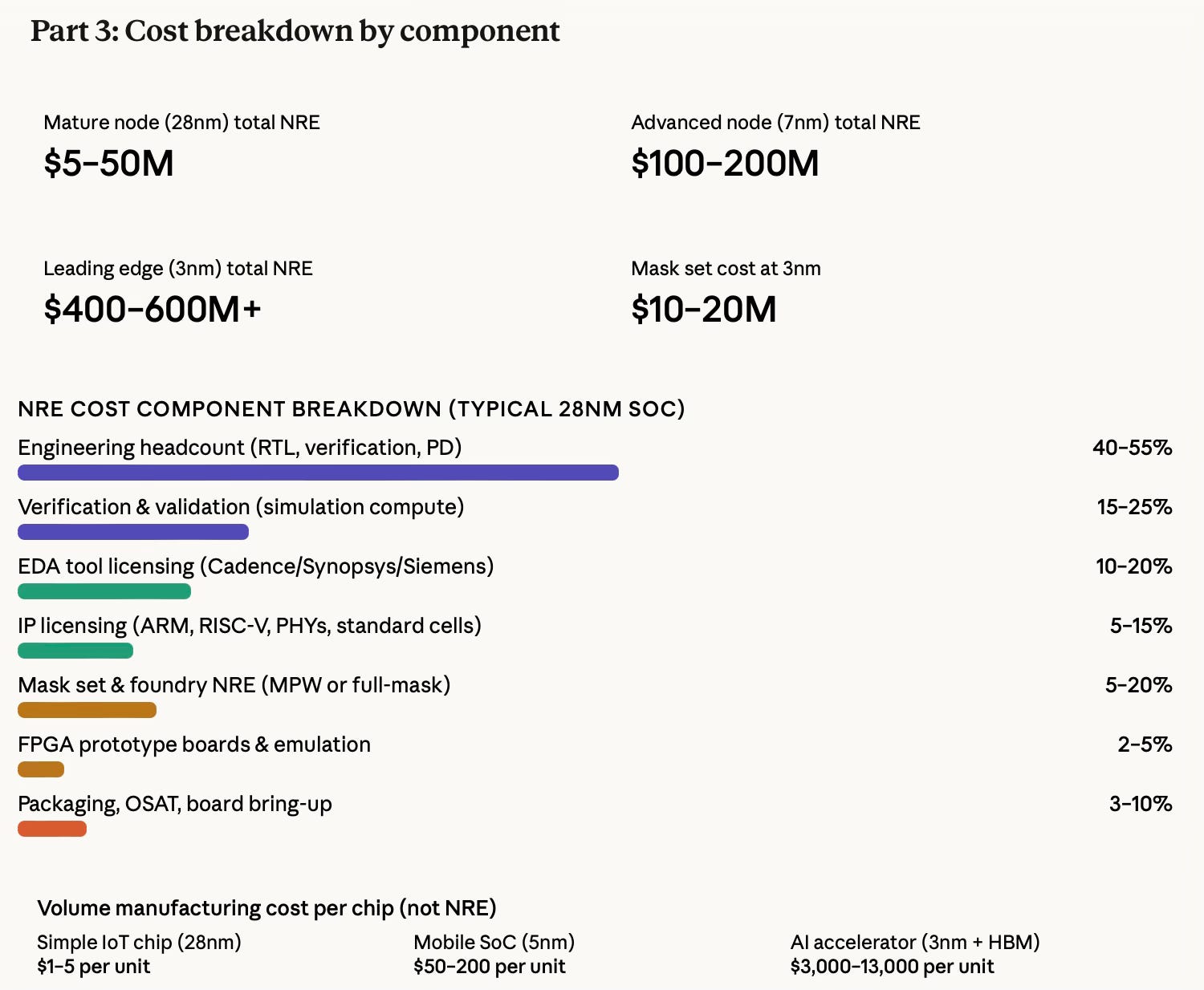
There are five stages in the chip development. Stage 1 is the drawing-board phase — what should the chip do, what architecture, what licensed IP blocks to buy. Stage 2 is where the actual design is written in code (RTL) and exhaustively simulated — this is the longest and most expensive phase of the entire lifecycle, absorbing 40–60% of all non-recurring engineering cost. Stage 3 is the FPGA sanity-check — running the design on a reprogrammable chip to shake out software and integration bugs before committing to expensive silicon. Stage 4 is tapeout — the design is frozen and handed to a foundry like TSMC, which etches it onto wafers using costly photomasks; any bug found here requires a full respin. Stage 5 is where the chip actually reaches customers — first in small pilot batches for qualification, then at scale, with economics that only work once volume is high enough to spread the NRE costs. The key insight connecting all five: each stage is a gate. A mistake at Stage 2 that slips through costs a hundred times more to fix at Stage 4, and a mistake at Stage 4 costs a year and tens of millions to fix at Stage 5.
India cannot replicate the US VC industry, at least for the foreseeable future. India’s angel funding industry does not invest in high-risk sectors like the chip design industry. Indian VCs are still at a seed stage ($1M-$3M) and cannot fund at the levels needed to succeed. Further, as mentioned earlier, VC funding in India for chip design is tiny compared to the requirement.
Nor does it have global companies that can offer commercialisation platforms for its startups. Further, global OEMs already have long-term partnerships with established and reliable chip design suppliers and will, therefore, be reluctant to experiment with a new chip designer. New chip design companies will also not be able to signal reliability in terms of meeting the massive volumes demanded by OEMs, the exacting standards and upgrade requirements, etc.
Given the aforesaid, it’s therefore not prudent to throw scarce public finance at startups purely in the hope that the demand-side (for these chip/product design startups) will emerge on its own after some time. The best use of scarce public funds in this context is to derisk and expand the envelope of private capital that might be interested in investing in risky chip design startups.
In the circumstances, one strategy would be to emulate parts of the Chinese playbook. There, the government supplemented the funding of startups with active market development interventions. However, there are limits to how much of it can be done in India, given the size of financing required (China is estimated to have spent $250 bn on the semiconductor chip industry) and the market-making efforts.
However, as a strategy, the Government of India could start by targeting 3-4 large-volume electronic products that are being procured by the government or are in demand in the Indian market. It can bring together promising (chip or product) design startups and product OEMs (and their manufacturing partners, EMCs). The OEMs could be supported to either buyout or license technology from the startups and adopt these domestic designs.
Electricity smart meters, surveillance cameras, fixed wireless access (FWA) devices, and automobile and heavy equipment chips are examples with very large domestic demand, where the aforesaid strategy can be pursued to catalyse domestically designed chips and OEMs. Unlike mobile phones or routers, these product markets are large enough and may have slightly lower entry barriers for domestic companies.
But this will require very high-level commitment and tight coordination by the central government, involving multiple departments, to integrate this strategy with public procurements, for market consolidation, mandating of product standards, expediting regulatory enablers and permissions, etc. Besides, the government must also work closely with private manufacturers and OEMs, even supporting them in their business development.
In the case of public procurements, this would involve effectively picking winners and giving them large multi-year contracts. For example, in the case of smart meters, the meter supply and O&M contractors (6-9 year TOTEX contracts) could be mandated to supply domestically designed and manufactured meters. They should be supported to bring together OEM/EMC and chip and product design startups. The support provided by the Ministry of Power for smart meter installations under the Atmanirbhar Bharat Scheme could be leveraged to catalyse domestic chip and meter design.
Surveillance camera manufacturers require regulatory approvals. These approvals could be linked to the use of domestically designed chips. This requirement can be gradually phased in to allow domestic design capabilities to emerge.
In conclusion, the best use of public policy to catalyse semiconductor chip design in India may be on the market-making side to complement the limited public funds to support startups.
No comments:
Post a Comment